HOME > Research Summaries > Visualization of Ion Distribution by the Chemical Imaging Sensor
Research Summaries

Visualization of Ion Distribution by the Chemical Imaging Sensor
Tatsuo Yoshinobu
Professor
Department of Biomedical Engineering, Graduate School of Biomedical Engineering
E-mail:![]()
1. Introduction
For the visualization of chemical species in the sample, labels such as fluorescent dyes are often utilized. For certain applications, however, toxicity of such dyes may be a problem. In this study, a label-free method of ion imaging based on a semiconductor device is developed.
Chemical sensors based on semiconductor devices are advantageous for miniaturization, integration and fabrication of various structures on their surfaces with the help of microfabrication techniques. A well-known semiconductor-based chemical sensor is the ion-sensitive field effect transistor (ISFET) [1, 2], which has the field effect structure or the electrolyte-insulator-semiconductor (EIS) structure. The ISFET is put to practical use, for example, in a portable pH meter. The EIS capacitive sensor [3] and the light-addressable potentiometric sensor (LAPS) [4] are other examples of chemical sensors based on the EIS structure. Figure 1 schematically compares the structures of these three sensors.
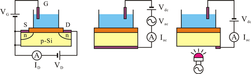
Fig.1 Structures of (a) ISFET, (b) EIS capacitive sensor and (c) LAPS.
Chemical sensors based on the EIS structure detect the change of the distribution of carriers in the semiconductor layer, which responds to the change of the ion concentration of the solution in contact with the sensing surface. The ISFET detects the change of the conductance of the channel between the source and the drain, whereas the EIS capacitive sensor and the LAPS detect the change of the capacitance of the depletion layer at the semiconductor-insulator interface.
Since the LAPS measures the photocurrent to detect the change of the capacitance of the depletion layer, spatially resolved measurement is possible by using a scanning laser beam.
2. Chemical imaging sensor
2.1. Principle
The chemical imaging sensor [5,6] is based on the measurement principle of the LAPS. At the semiconductor-insulator interface of the chemical imaging sensor, the width of the depletion layer is spatially distributed reflecting the spatial distribution of the ion concentration on the sensing surface. When the sensor plate is illuminated with a focused laser beam modulated at a certain frequency, an ac photocurrent is generated with an amplitude dependent on the local value of the capacitance of the depletion layer at the illuminated position. Therefore, the photocurrent image obtained by scanning the sensor plate with a focused laser beam gives a map of the ion concentration on the sensing surface.
The spatial resolution of the chemical imaging sensor is determined by parameters such as the diameter of the focused laser beam, the thickness of the semiconductor layer and the diffusion length of minority carriers in the semiconductor layer. A 5-μm line-and-space pattern was already resolved, and further improvement of the spatial resolution up to 1μm is expected by using a-Si thin film.
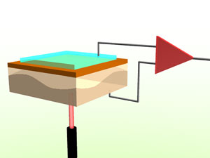
Fig.2 Principle of the chemical imaging sensor. The photocurrent is dependent on the width of the depletion layer, which is distributed in response to the spatial distribution of the ion concentration on the sensing surface.
2.2. Application
Possible applications of the chemical imaging sensor include visualization of electrochemical reactions and observation of biological specimens.
Figure 3 shows an example of the visualization of an electrochemical system. The temporal change of the pH distribution between two parallel electrodes is due to the diffusion of ions after electrolysis. By using the chemical imaging sensor, direct observation and quantitative analysis of reaction and diffusion are possible.
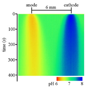
Fig.3 Observation of the pH distribution between two electrodes.
Figure 4 is an example of the visualization of biological specimens. In this example, the proximity of an E. coli colony cultured on agar is acidified due to the metabolic activity. By using the chemical imaging sensor, biological activities can be measured visually and quantitatively.
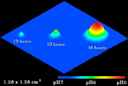
Fig.4 Observation of an E. coli colony cultured on agar.
3. Prospects
In order to develop the applications of the chemical imaging sensor, following aspects of the chemical imaging sensor must be studied.
(1) Performance
For the precise detection of smaller structures, the spatial resolution and the S/N ratio of the chemical imaging sensor must be improved. High-speed measurement is necessary for dynamic measurement.
(2) Multisensor
By modifying the sensing surface, distributions of various chemical species other than protons (pH) can be also visualized. Multisensors can be built by integrating membranes with sensitivities to different chemical species on a single sensor plate.
(3) Large-area sensor
For the measurement of large specimens, large-area sensors and scanners must be developed. For the scanning of a large area, reduction of the measuring time is important, for example, by using more than one light source for the scan.
(4) Application to microfluidic devices
By constructing microchannels on the sensing surface, the distribution of the chemical species inside the channel can be visualized.
References
[1] Bergveld P. Development of an ion-sensitive solid-state device for neurophysical measurements. IEEE Trans. Biomed. Eng. BME-17, 70, 1970.
[2] Matsuo T. Wise KD. An integrated field-effect electrode for biopotential recording. IEEE Trans. Biomed. Eng. BME-21, 485-487, 1974.
[3] Schoning MJ, Poghossian A, Yoshinobu T, Luth H. Semiconductor-based field-effect structures for chemical sensing. SPIE Proc. 4205, 188-198, 2001.
[4] Hafeman DG, Wallace Parce J, McConnel HM, Light-addressable potentiometric sensor for biochemical systems. Science 240, 1182-1185, 1988.
[5] Nakao M, Yoshinobu T and Iwasaki H. Scanning-laser-beam semiconductor pH-imaging sensor. Sensors and Actuators B 20, 119-123, 1994.
[6] Yoshinobu T, Iwasaki H, Ui Y, Furuichi K, Ermolenko Yu, Mourzina Yu, Wagner T, Nather N, Schoning MJ. The light-addressable potentiometric sensor for multi-ion sensing and imaging. Methods 37, 94-102, 2005.